service - MicroED
B A C KBridging the Gap in Crystal Size
MicroED is a new technology, which uses electron as incident beam to obtain MicroED microcrystalline electron diffraction data on Cryo-TEM.
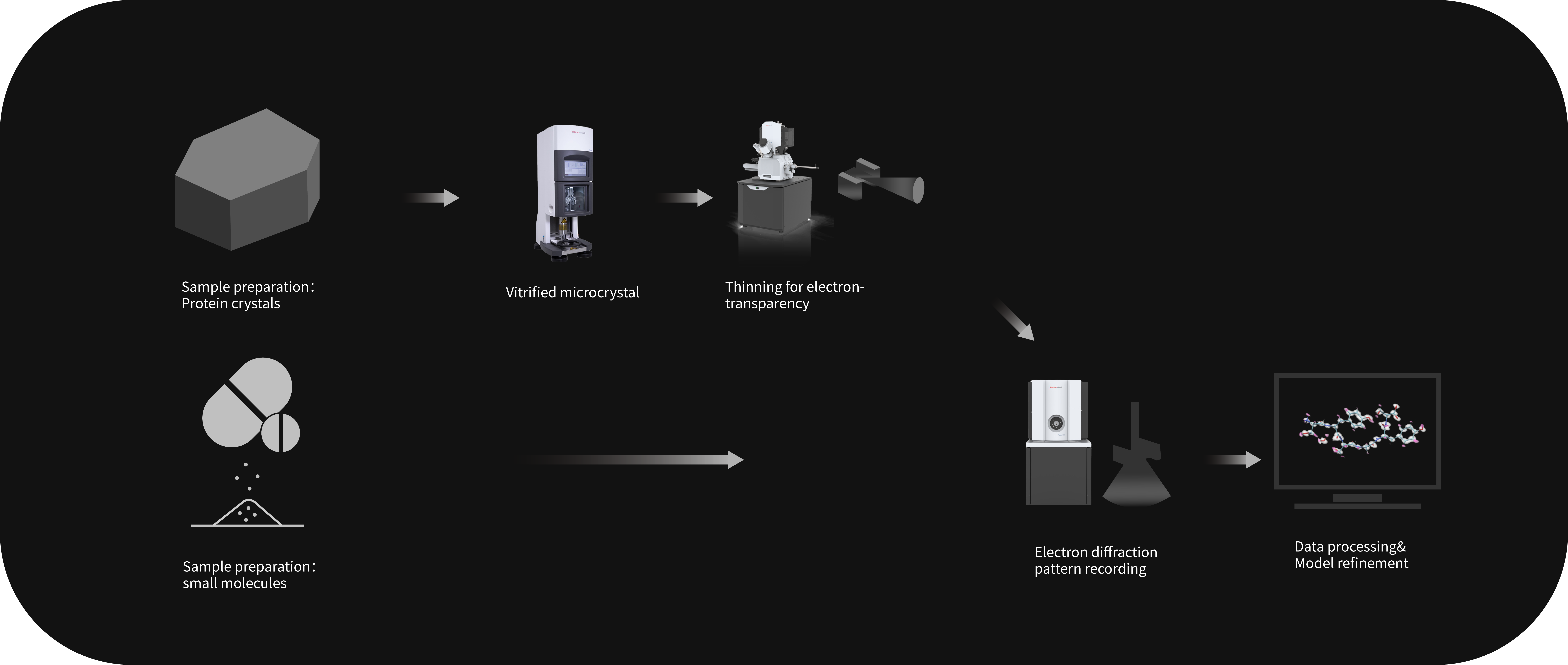
Electrons interact with matter more strongly than X-rays. This means that MicroED may be used to solve structures from vanishingly small crystals(100–300 nm), but also implies that larger crystals (>1 um thick) cannot be efficiently penetrated by the electron beam. However, larger crystals can be thinning to appropriate thickness using focused ion beam (FIB) milling technique. Alleviating the need for large and high-quality crystal growth, MicroED is amenable to examine both crystals much smaller than the size typically needed for X-ray crystallography and larger crystals.


MicroED Workflow

Why choose MicroED?
● A powerful tool in resolve small molecule structures.
● Reduced requirement for large crystals.
● High or ultrahigh resolution for small molecule.
● Higher speed in structure determination.
● Lower costs in structure determination.
Why choose ShuimuBio for MicroED?
● We can not only determine high resolution structures for challenging small molecule, peptide, but also for macromolecular samples by MicroED.
● We have world-class experts in the research and applicaiton of MicroED.
● We delivered about 80% of MicroED projects with resloution about 0.6~1.0Å.

About the samples
Crystals Size:
small molecule or peptide crystal: 100–300 nm
protein crystal: 100 nm-100 μm